Abstract :
[en] Silver nanowire (AgNW) networks are widely considered as a key class of transparent conductive materials for next-generation flexible and stretchable electronics. Their compatibility with solution-based processing, combined with excellent optical and electrical performance, makes them suitable for large-area, low-cost device integration. However, due to their geometry, AgNW are inherently susceptible to electrical instabilities [1,2]. In particular, their small cross-sections can lead to significantly high current densities, raising concerns about failure mechanisms such as electromigration, localized Joule heating, or junction degradation under electrical stress.
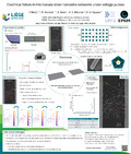
In this work, we investigate electrical transport in micrometer-sized AgNW networks, ranging from 20 to 30 µm in width, comprising only a few nanowires per conductive path. These microscale networks serve as model systems to study failure mechanisms under pulsed voltage stress. By applying a sequence of voltage pulses of increasing amplitude up to breakdown, generally up to 1 V, we observe the evolution of the network resistance and identify the locations of electrical failure, typically linked to the most stressed junctions or nanowire segments.
To rationalize these observations, each experimental network is mapped to an equivalent electrical circuit, accounting for segment resistances, junction resistances and contact resistances with electrodes. Numerical simulations based on this digital twin circuit allow us to compute local current densities and predict failure-prone zones. The comparison between experimental failure locations and simulated stress maps enables iterative refinement of key parameters, improving the predictive power of the model. In particular, this comparison allows us to extract parameters such as the resistance of AgNW junctions, the critical current density at which failure occurs, and characteristic features of the resulting break morphology.
While the present work focuses on small-scale networks, this methodology lays the groundwork for simulating larger, more realistic AgNW systems involving tens of thousands of nanowires. Such predictive tools are essential for optimizing the design and reliability of transparent conductive architectures, particularly in emerging transparent and flexible device platforms.
[1] M. Lagrange et al 2017 Nanotechnology 28 055709
[2] M. Waliullah and R. A. Bernal 2022 Nanotechnology 33 305706